Measurements are at the heart of science, and the quality of equipment dictates the quality of our measurements. In the Hollen Lab, a condensed matter physics lab at the University of New Hampshire, we measure the electronic and physical properties of next-generation materials. An emerging class of two-dimensional (2D) materials, which consist of a single atomic layer, are especially interesting because of their exceptional mechanical strength and adjustable electronic properties. These materials are promising for use in a wide range of applications, such as electronic devices, anti-corrosion coatings, and medical sensors, among others. Understanding the properties of these materials helps engineers integrate them into future technologies.

We study these materials using a scanning tunneling microscope (STM), an extremely high-resolution microscope that lets us see the atoms that make up the surface of the material. To get high-quality images at atomic resolution, the microscope’s metallic probe (also referred to as a tip), which is a wire that scans the sample surface, needs to be very sharp—ideally with a single atom at the probe’s apex. My research project, which was funded by an Undergraduate Research Award (URA) through the Hamel Center for Undergraduate Research, focused on understanding how the shape, uniformity, and sharpness of the STM probe affects its interaction with semiconducting samples. Understanding these probe-sample interactions helps us correctly interpret the images acquired with the STM. In particular, it helps us differentiate between features in the image that result from inherent properties of the material, like a topographical bump, and features resulting from the material’s interaction with the STM probe.

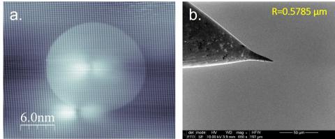
Figure 1: a. STM surface image of black phosphorus, a 2D semiconductor, showing a bright halo around a dumbbell shaped defect in the material (Taken by Jake Riffle of Hollen Lab). b. SEM image of an STM probe I produced using my setup. R stands for the radius of curvature, or how sharp the probe is at the apex.
A good example of a non-inherent feature is a bright halo that appears around defects in the material (like impurities or missing atoms) when we image semiconductors (Figure 1a). This halo feature arises from a phenomenon called tip-induced band bending, where the strong electric field between the probe and sample induces a change in the electronic properties of the sample. With this phenomenon in mind, we interpret the halo-like feature as an electronic signature resulting from interactions with the STM probe rather than an inherent surface contour.
For my project, I built a specialized etching setup to produce sharp STM probes of different shapes from platinum-iridium wire. The setup used an electricity-driven chemical reaction to carve at the probe wire and shape it. I used a scanning electron microscope (SEM), which is used to look at nanometer-to-micrometer-scale objects like carbon nanotubes and red blood cells, to image the produced probes (Figure 1b). Probes fabricated with my setup and procedure successfully produced high-resolution STM images. As a result of this portion of my research, the Hollen Lab now has the capability of making sharp platinum-iridium probes, which improve the quality of STM imaging in the lab.

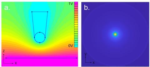
Figure 2: a. FEMM simulation of the electric-potential field between the probe (surrounded by light blue), and the 2D sample (surrounded by pink). This is a side view of how an STM operates. b. Top-down view of a., constructed with a MATLAB program I wrote. This simulated image can be easily compared to experimentally acquired STM images, as both have a top-down orientation.
To explore the phenomenon of probe-induced band bending and understand the shape of the resulting halo-like feature, I modeled probes with different cross-sectional symmetries and simulated the electric field produced by them. The initial modeling and simulation were done in Finite Element Method Magnetics (FEMM), a software used to solve electromagnetic problems in two-dimensions. Since FEMM only simulates the STM setup of a probe and a sample from a side view (Figure 2a), I wrote a MATLAB program that creates a top-down view (Figure 2b), which can be easily compared to STM images. In this portion of the research, I found that a circularly symmetric probe creates a circularly symmetric electric field, as shown in Figure 2b. From this we infer that the halo around defects in the material would be perfectly circular. Currently, I am exploring the effects of a probe with two or more different cross-sectional symmetries. To do this, I change the shape of the probe’s apex in the FEMM program.
In the future, I hope to generalize the simulation to non-symmetric probes. This will yield more-practical results than the perfectly symmetric case, as probes produced in the lab typically are not perfectly symmetric. Then, I will model specific STM probes that I made and compare simulation results to real STM images taken with these probes. This will help us determine whether the electric field from the probe is the only factor in producing the halo-like feature, or whether there are other inherent properties of the material that we should consider.
I would like to thank Dr. Shawna Hollen for being a wonderfully supportive and attentive mentor and for guiding me throughout the project, from writing the proposal to publishing the results. I’d also like to thank Ph.D. candidate Jake Riffle for his valuable advice and help with programming. I am thankful for my fruitful collaborations with the kind Dr. Sara Mueller, Ph.D. candidates Steven Arias and Robert Wacko, and Dr. Victor Brar, in assembling the probe-fabrication setup. The University Instrumentation Center has trained me to use the SEM with patience and professionalism, and for that I am also grateful. Finally, I’d like to give my gratitude to the Hamel Center for Undergraduate Research and to Mr. Dana Hamel, whose financial contributions as part of the URA award made this research possible.
Copyright 2021, Lihy-Eden Buchbinder
